- 您现在的位置:买卖IC网 > Sheet目录2005 > LTC2242IUP-10#PBF (Linear Technology)IC ADC 10BIT 250MSPS 64-QFN
LTC2242-10
5
224210fd
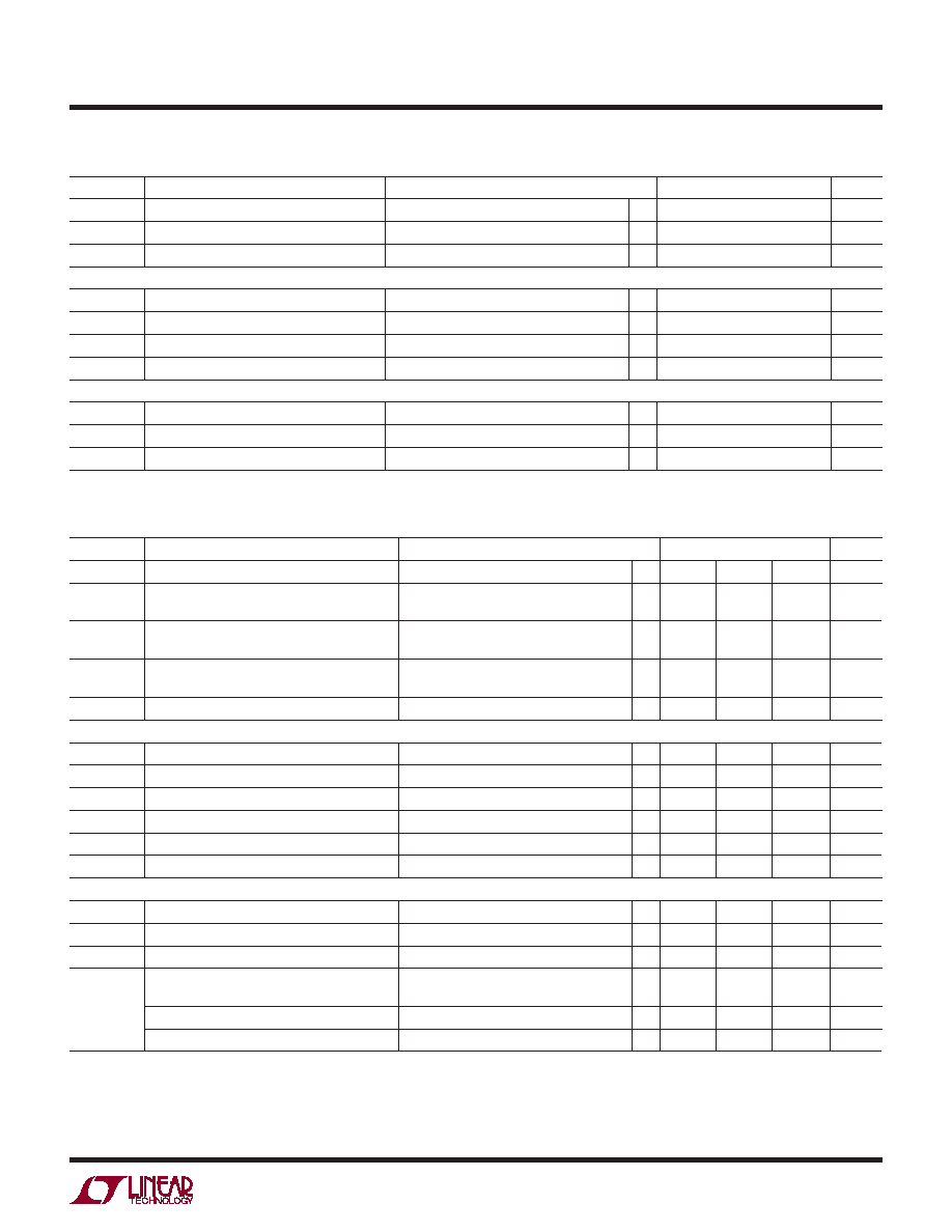
power requireMenTs
SYMBOL
PARAMETER
CONDITIONS
MIN
TYP
MAX
UNITS
VDD
Analog Supply Voltage
(Note 8)
●
2.375
2.5
2.625
V
PSLEEP
Sleep Mode Power
SHDN = High, OE = High, No CLK
1
mW
PNAP
Nap Mode Power
SHDN = High, OE = Low, No CLK
28
mW
LVDS OUTPUT MODE
OVDD
Output Supply Voltage
(Note 8)
●
2.375
2.5
2.625
V
IVDD
Analog Supply Current
●
285
320
mA
IOVDD
Output Supply Current
●
58
70
mA
PDISS
Power Dissipation
●
858
975
mW
CMOS OUTPUT MODE
OVDD
Output Supply Voltage
(Note 8)
●
0.5
2.5
2.625
V
IVDD
Analog Supply Current
(Note 7)
●
285
320
mA
PDISS
Power Dissipation
740
mW
The ● denotes the specifications which apply over the full operating temperature
range, otherwise specifications are at TA = 25°C. (Note 9)
TiMing characTerisTics The
●
denotes the specifications which apply over the full operating temperature
range, otherwise specifications are at TA = 25°C. (Note 4)
SYMBOL
PARAMETER
CONDITIONS
MIN
TYP
MAX
UNITS
fS
Sampling Frequency
(Note 8)
●
1
250
MHz
tL
ENC Low Time (Note 7)
Duty Cycle Stabilizer Off
Duty Cycle Stabilizer On
●
1.9
1.5
2
500
ns
tH
ENC High Time (Note 7)
Duty Cycle Stabilizer Off
Duty Cycle Stabilizer On
●
1.9
1.5
2
500
ns
tAP
Sample-and-Hold Aperture Delay
0.4
ns
tOE
Output Enable Delay
(Note 7)
●
5
10
ns
LVDS OUTPUT MODE
tD
ENC to DATA Delay
(Note 7)
●
1
1.7
2.8
ns
tC
ENC to CLKOUT Delay
(Note 7)
●
1
1.7
2.8
ns
DATA to CLKOUT Skew
(tC – tD) (Note 7)
●
–0.6
0
0.6
ns
Rise Time
0.5
ns
Fall Time
0.5
ns
Pipeline Latency
5
Cycles
CMOS OUTPUT MODE
tD
ENC to DATA Delay
(Note 7)
●
1
1.7
2.8
ns
tC
ENC to CLKOUT Delay
(Note 7)
●
1
1.7
2.8
ns
DATA to CLKOUT Skew
(tC – tD) (Note 7)
●
–0.6
0
0.6
ns
Pipeline
Latency
Full Rate CMOS
5
Cycles
Demuxed Interleaved
5
Cycles
Demuxed Simultaneous
5 and 6
Cycles
发布紧急采购,3分钟左右您将得到回复。
相关PDF资料
LTC2245IUH#TRPBF
IC ADC 14BIT 10MSPS 3V 32-QFN
LTC2249IUH#TRPBF
IC ADC 14BIT 80MSPS LP 32-QFN
LTC2251IUH#PBF
IC ADC 10-BIT 125MSPS 3V 32-QFN
LTC2253IUH#TRPBF
IC ADC 12BIT 125MSPS 3V 32-QFN
LTC2255CUH#TRPBF
IC ADC 14BIT 125MSPS 3V 32-QFN
LTC2258IUJ-12#PBF
IC ADC 12BIT 65MSPS 1.8V 40-QFN
LTC2262CUJ-14#TRPBF
IC ADC 14BIT 150MSPS 40-QFN
LTC2262IUJ-12#PBF
IC ADC 12BIT 150MSPS 40-QFN
相关代理商/技术参数
LTC2242IUP-10#TRPBF
功能描述:IC ADC 10BIT 250MSPS 64-QFN RoHS:是 类别:集成电路 (IC) >> 数据采集 - 模数转换器 系列:- 标准包装:1 系列:- 位数:14 采样率(每秒):83k 数据接口:串行,并联 转换器数目:1 功率耗散(最大):95mW 电压电源:双 ± 工作温度:0°C ~ 70°C 安装类型:通孔 封装/外壳:28-DIP(0.600",15.24mm) 供应商设备封装:28-PDIP 包装:管件 输入数目和类型:1 个单端,双极
LTC2242IUP-10-PBF
制造商:LINER 制造商全称:Linear Technology 功能描述:10-Bit, 250Msps ADC
LTC2242IUP-10-TR
制造商:LINER 制造商全称:Linear Technology 功能描述:10-Bit, 250Msps ADC
LTC2242IUP-10-TRPBF
制造商:LINER 制造商全称:Linear Technology 功能描述:10-Bit, 250Msps ADC
LTC2242IUP-12
制造商:Linear Technology 功能描述:ADC Single Pipelined 250Msps 12-bit Parallel/LVDS 64-Pin QFN EP 制造商:Linear Technology 功能描述:MS-ADC/High Speed, 12-bit, 250Msps ADC
LTC2242IUP-12#PBF
制造商:Linear Technology 功能描述:ADC Single Pipelined 250Msps 12-bit Parallel/LVDS 64-Pin QFN EP 制造商:Linear Technology 功能描述:Single ADC Pipelined 250Msps 12-bit Parallel/LVDS 64-Pin QFN EP 制造商:Linear Technology 功能描述:IC ADC 12BIT 250MSPS 64-QFN 制造商:Linear Technology 功能描述:A/D Converter (A-D) IC 制造商:Linear Technology 功能描述:IC, ADC, 12BIT, 250MSPS, QFN-64, Resolution (Bits):12bit, Sampling Rate:250MSPS, Supply Voltage Type:Single, Supply Voltage Min:2.375V, Supply Voltage Max:2.625V, Supply Current:285mA, Digital IC Case Style:QFN, No. of Pins:64 , RoHS Compliant: Yes 制造商:Linear Technology 功能描述:MS-ADC/High Speed, 12-bit, 250Msps ADC
LTC2242IUP-12#TRPBF
制造商:Linear Technology 功能描述:ADC Single Pipelined 250Msps 12-bit Parallel/LVDS 64-Pin QFN EP T/R 制造商:Linear Technology 功能描述:IC ADC 12BIT 250MSPS 64-QFN
LTC2242UP-10
制造商:LINER 制造商全称:Linear Technology 功能描述:10-Bit, 250Msps ADC